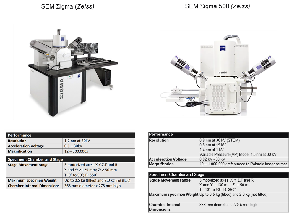
Scanning Electron Microscopes (SEMs) employed in the MM section are Field Emission Gun (FEG) systems, which administers an electron beam controlling its focus using magnetic lenses and interchangeable beam intensity to provide advanced analytics. The electron beam can be manipulated in the range 0.1 to 30 keV providing a resolution of up to nanometric resolution.
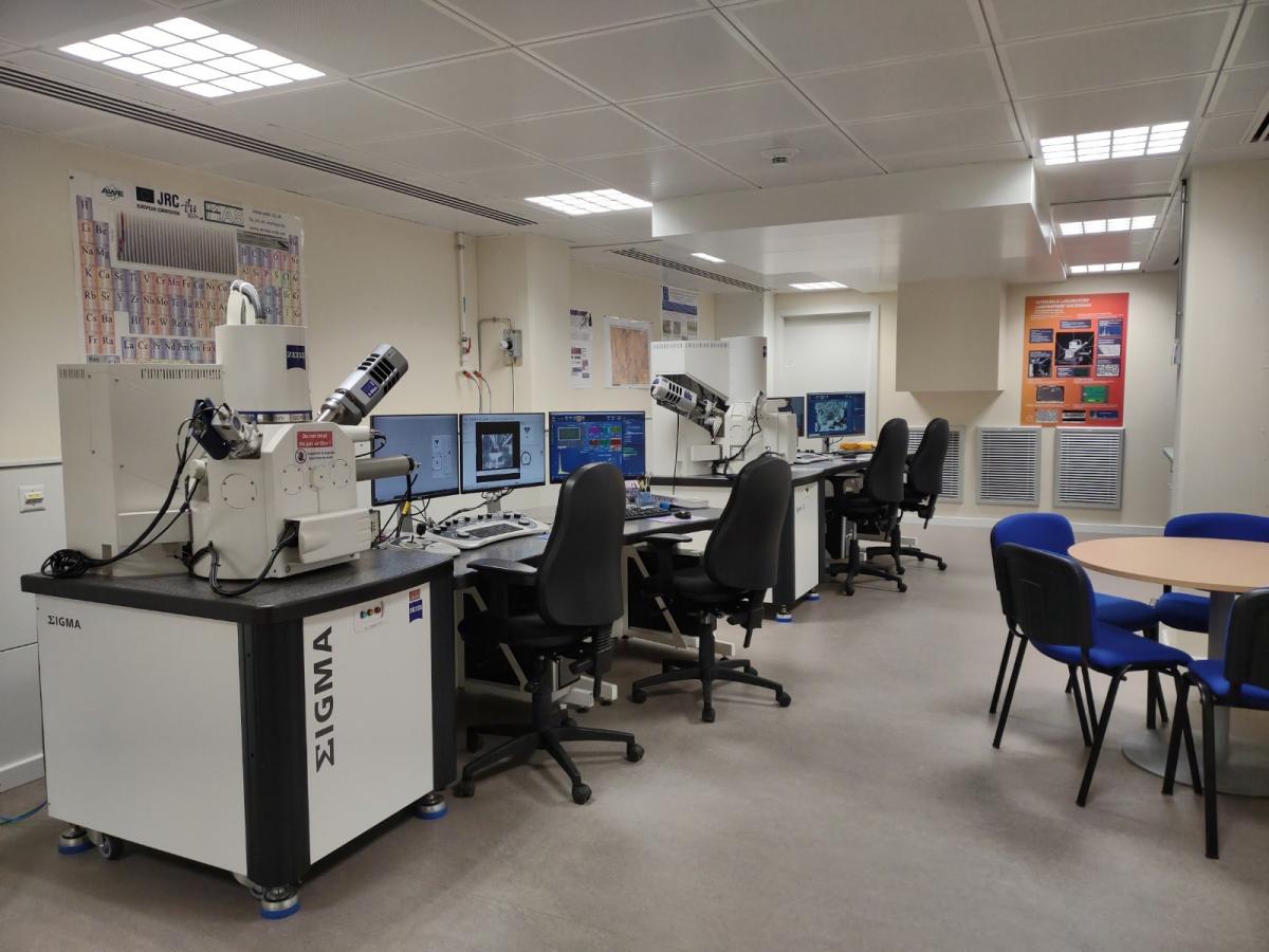
Two SEM systems are available Sigma and Sigma-500 from ZEISS.
Detectors available:
- Secondary Electron Emission Detector (SE2) - Topographical imaging
- Backscattered Electron Imaging Detector (AsB)- Atomic weight contrast imaging
- Inlens Duo Detector (Inlens) - High resolution topographical imaging
- X-max Energy Dispersive X-ray Spectroscopy (EDX) Detector - Chemical analysis
- Electron Backscattered Diffraction (EBSD) Detector - Crystallographic material analysis
- X-max Extreme Detector - Chemical analysis with an extreme light element sensitivity including detection of lithium
Systems capabilities:
- Topographical and morphological inspection of specimens with wide ranging depths of field
- Compositional contrast and pollution studies
- Qualitative and semi-quantitative elemental analysis and elemental mapping
- Elemental analysis with ultimate spatial resolution (nanometric scale) at low-voltage
- Automatic Particle Analysis (APA) for particle analysis (thousands of particles can be characterized and classified by size and composition)
- Texture, phase, microstructural and deformation maps
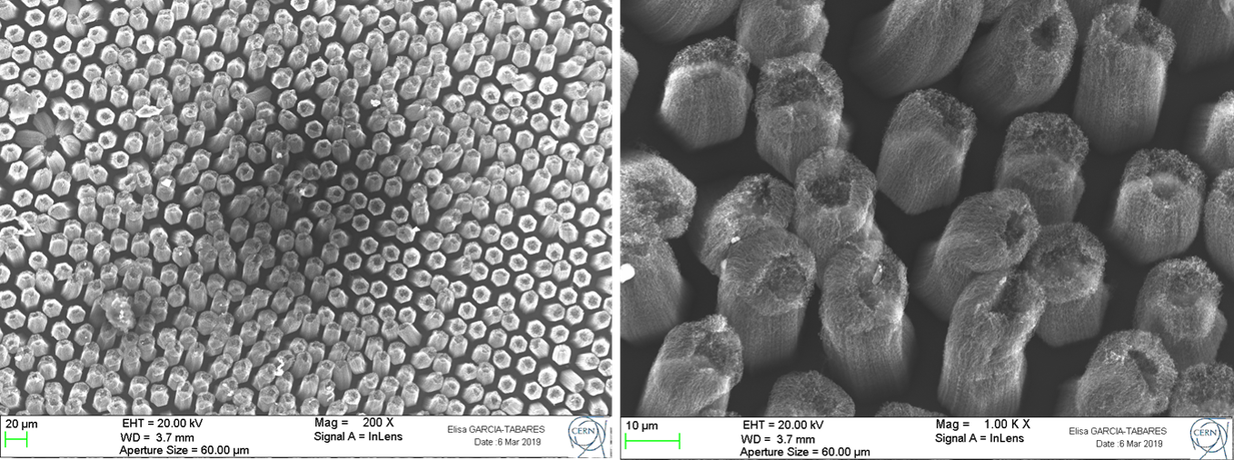
Morphological inspection of carbon nanotubes arrays for electron field emitters
Further information and technical specifications can be found here: SEM Sigma, SEM Sigma 500 and Extreme Detector
SEM room in 376/R-010