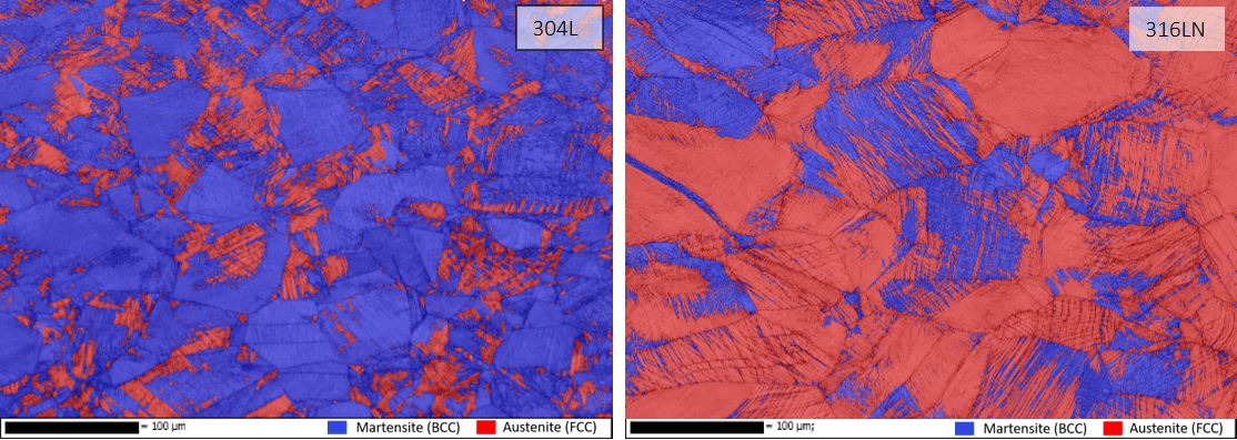
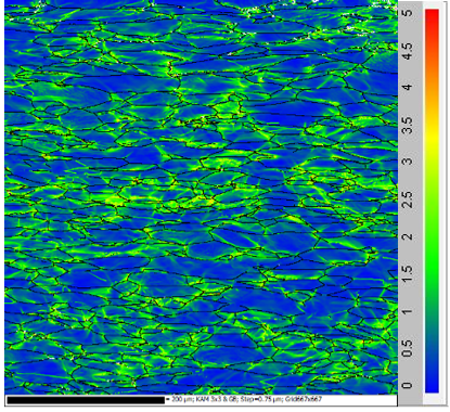
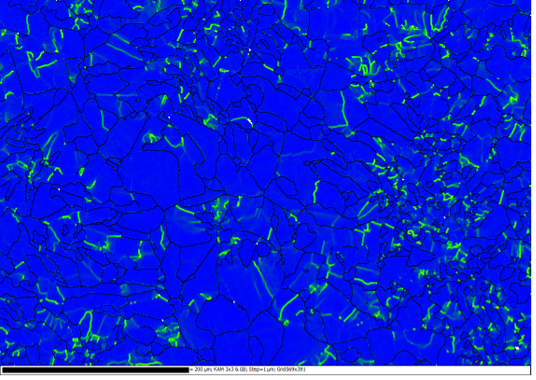
Electron Backscattered Diffraction (EBSD) is used to perform qualitative and quantitative microstructural analysis in the Scanning Electron Microscope (SEM), on a millimetre to a nanometre scale. It is one of the most advanced techniques within the repertoire of the microscopy team. It is a highly effective complimentary technique to other qualitative principles including X-Ray Diffraction (XRD) and Light Microscopy.
In essence, incident backscattered electrons are diffracted off the surface of a sample tilted to 70°. These electrons are collected by a phosphorus screen in a diffraction pattern arrangements called ‘Kikuchi bands’ characteristic to the samples specific structure and crystallographic orientations.
This technique is non-destructive and can be applied to crystalline, conductive materials with flat surface (normally polished) in order to investigate:
- Texture
- Grain size and orientation
- Tracking of phase transformations and segregation studies
- Recrystallisation studies
- Distribution local misorientations and twin boundary formations
 |
 |
 |